
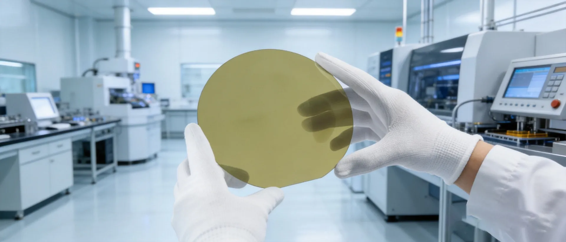
Global-leading SiC seed crystal bonding, automatic spin coating, wafer cleaning, hot press furnace, and Solid SiC ultrasonic machining systems. Empowering the semiconductor industry with innovative equipment solutions — over 90% global market share in key segments.
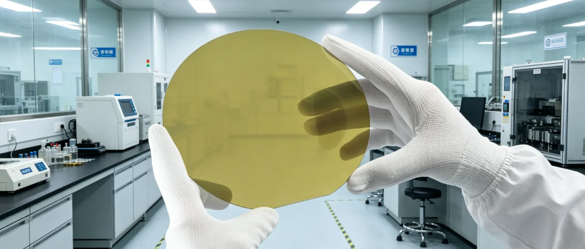
Industry-leading Solid SiC ultrasonic machining technology with zero sub-surface micro-crack defects. 40-150% efficiency improvement over traditional grinding. Serving global semiconductor manufacturers with precision SiC processing equipment.
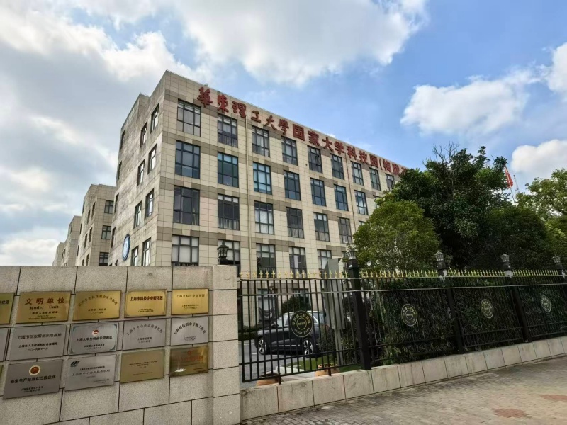
Shanghai Yangmi is a globally-oriented professional equipment manufacturer that empowers the semiconductor industry. With years of deep industry experience, we have built a comprehensive talent pool of 32 R&D designers, 80 production engineers, and 40 marketing and management professionals — a team of 152 professionals.
Our multi-location collaborative ecosystem spans: Global headquarters in Shanghai, a 20,000㎡ standardized production base in Hebei, and a self-built semiconductor industrial park in Jiangsu serving as our Asia-Pacific R&D headquarters and core semiconductor component production base.
Shanghai HQ + Hebei Production + Jiangsu R&D Park
Multiple world-first technologies, 32-person R&D team
Serving semiconductor fabs worldwide with dedicated support
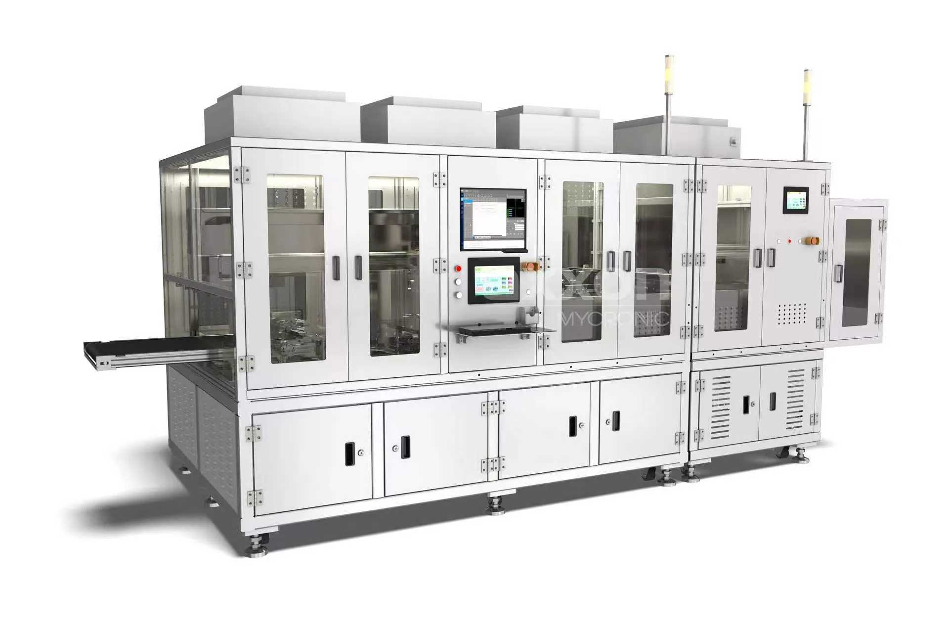
5 product lines covering bonding, coating, cleaning, thermal & machining
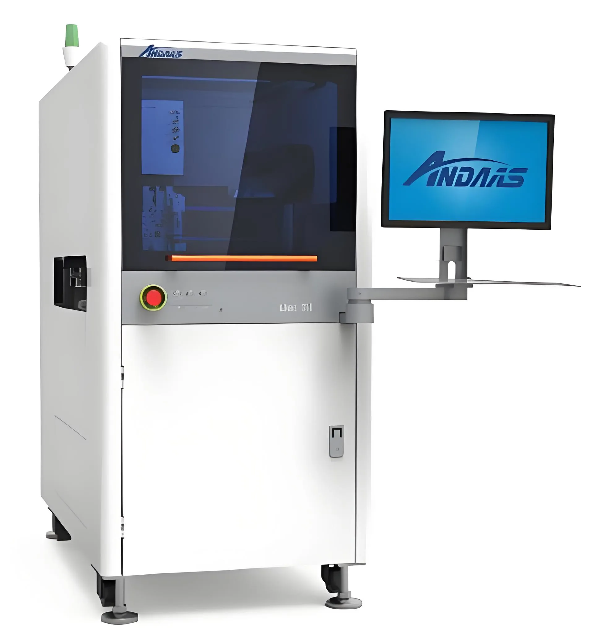
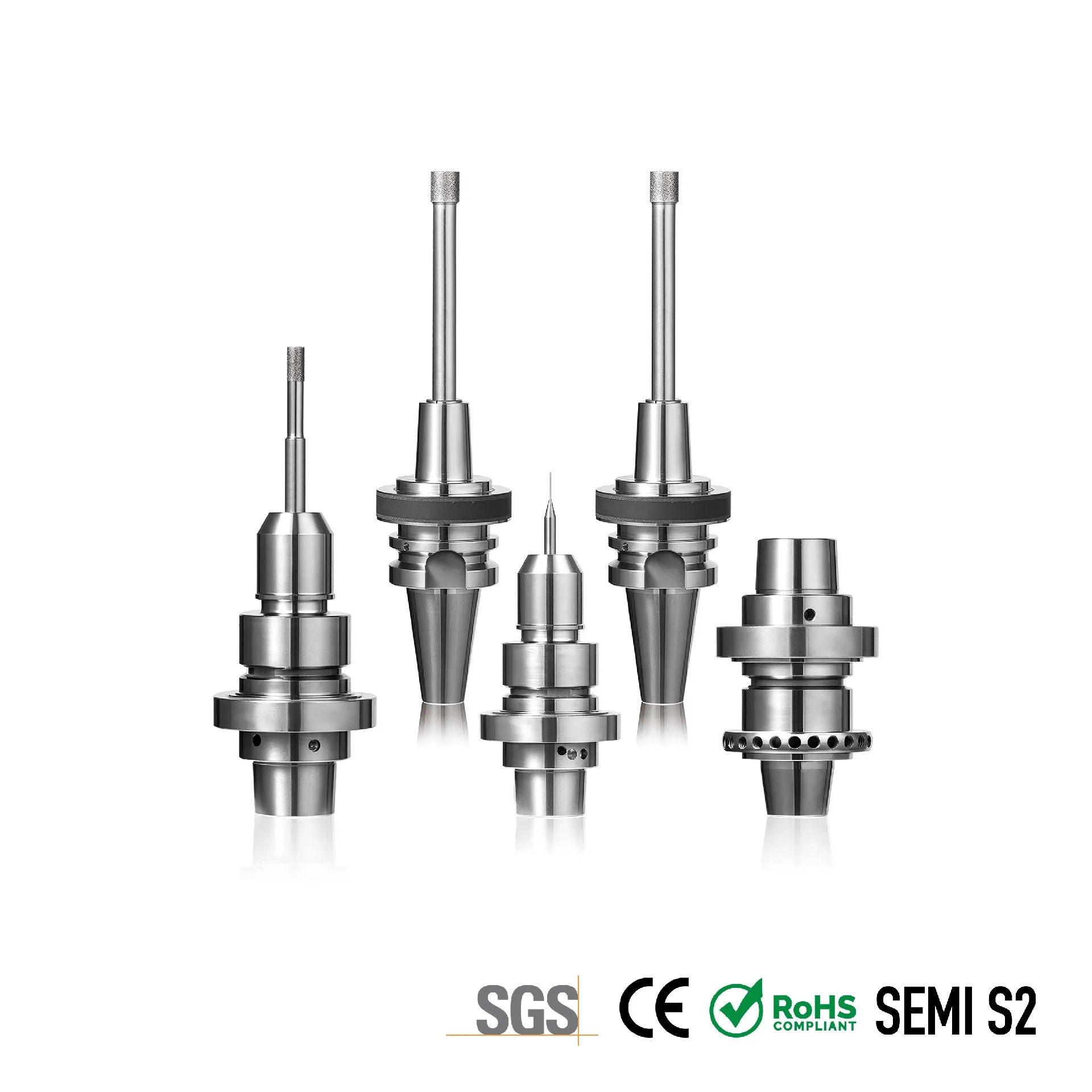
Solid SiC ultrasonic processing equipment: solves material stress-induced chipping, eliminates subsurface microcracks, reduces hole chipping to ≤0.03mm, increases processing efficiency by 40%~150%, extends PCD drill bit life by 100%~160%, halves the cost per tool, and ensures hole diameter fluctuation of ≤
Learn More →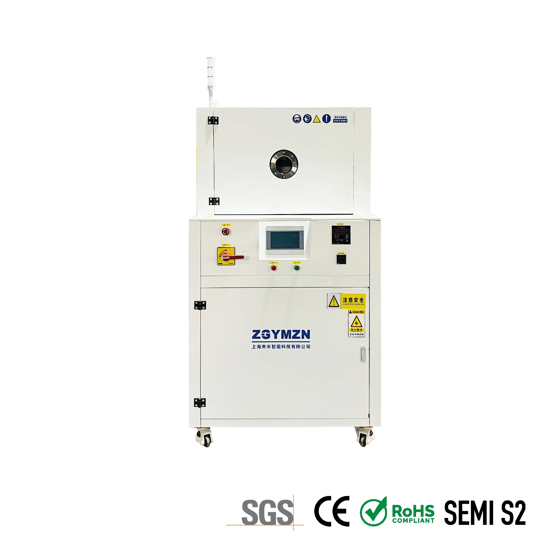
High-temperature bonding hot press furnace: It adopts a precise temperature control, pressure and vacuum control system to achieve uniform high-temperature bonding of various substrate materials.
Learn More →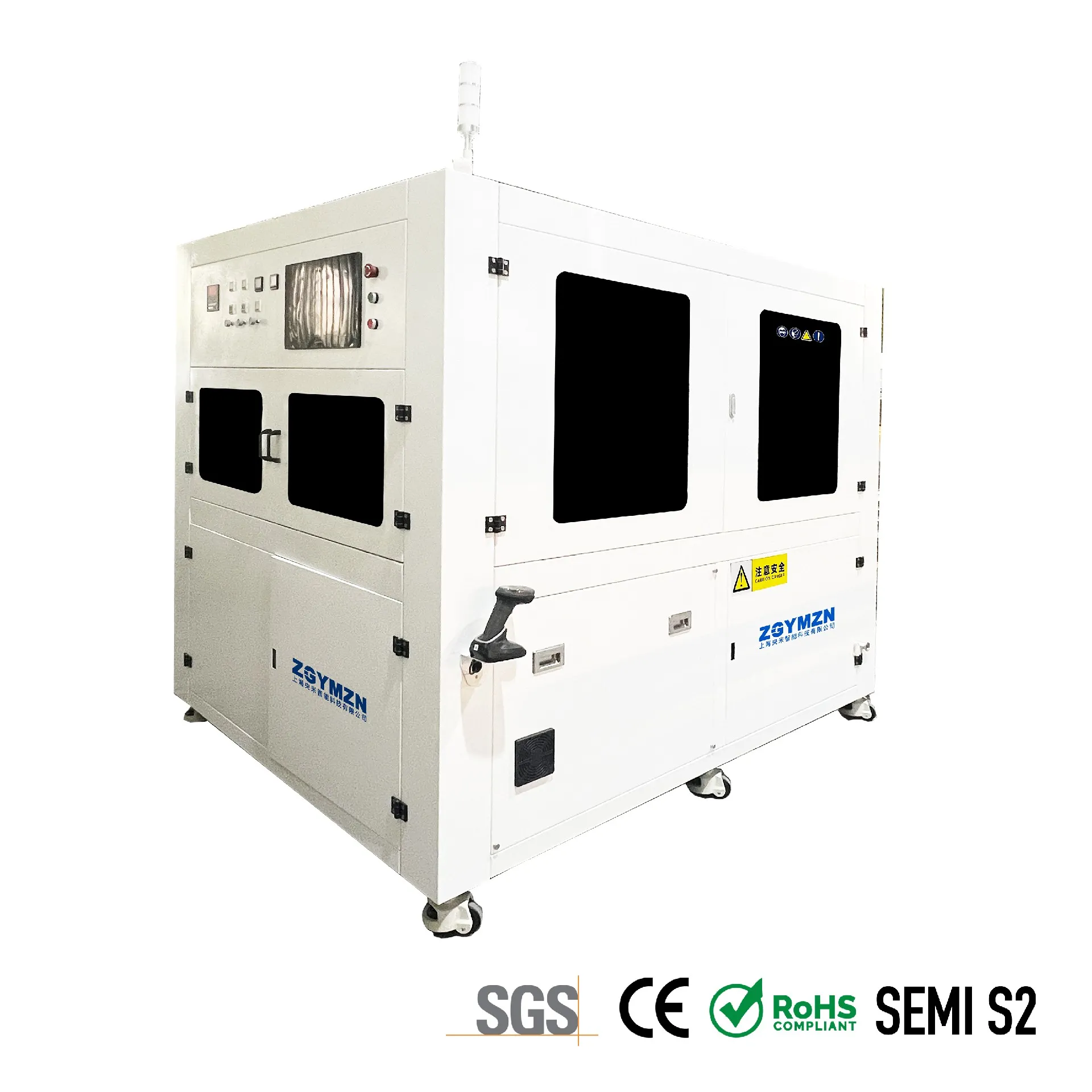
Automatic glue spraying/spreading: The fully automatic glue spraying machine can spray glue on substrate materials of various shapes. It is suitable for deep hole TSV spraying, high aspect ratio step spraying, and curing process. The fully automatic spreader can prepare various circular substrate ma
Learn More →Multiple globally pioneering technologies with over 90% market share in key semiconductor equipment segments.
32 R&D designers, 80 production engineers — full capability from design to manufacturing and after-sales support.
Large-scale standardized production base in Hebei plus self-built semiconductor industrial park in Jiangsu.
Shanghai global HQ, Hebei manufacturing center, Jiangsu Asia-Pacific R&D headquarters — full-chain coverage.
SiC and GaN device manufacturing
Micro-device precision fabrication
Wafer-level process equipment
Precision bonding and coating
LED / OLED / QLED manufacturing
High-reliability ceramic substrates
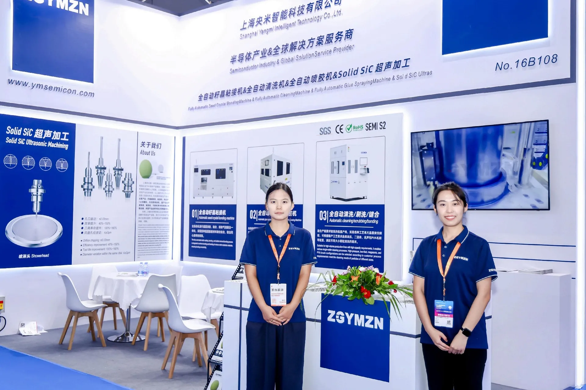
The semiconductor industry is at a critical juncture of rapid iteration, with material innovation and equipment localization being the core driving forces for its development. Shanghai Yangmi, with a global perspective, deeply cultivates the entire semiconductor industry chain, adheres to technological breakthroughs and product innovation, and is committed to providing the industry with stable, efficient, and domestically produced process equipment and overall solutions, contributing to the self-reliance and controllability of the semiconductor manufacturing industry chain.
Read More →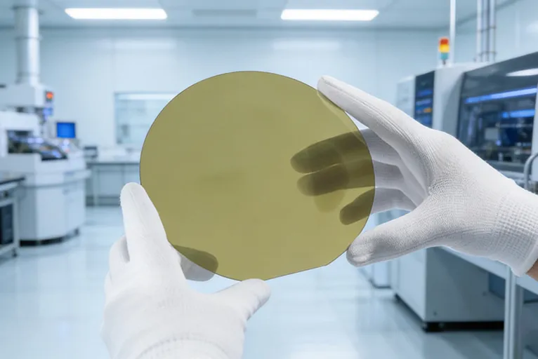
The silicon carbide (SiC) industry chain continues to mature, with substrate, epitaxial, and device manufacturing processes constantly iterating and large-size wafer capacity expanding, driving a steady decline in overall device costs and continuously broadening application boundaries. In the future, as the reliability of automotive-grade and industrial-grade products further improves, SiC will penetrate more high-power applications, providing fundamental material support for global green energy and high-end manufacturing.
Read More →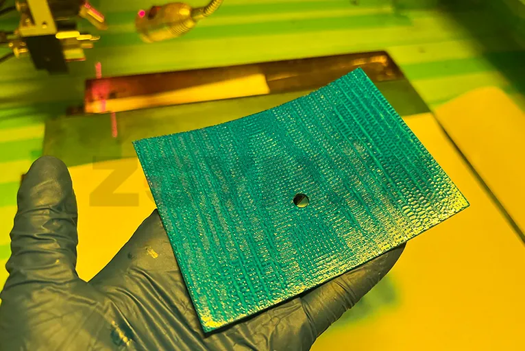
With the advancement of power semiconductors, with the iterative upgrades of MEMS microdevices and precision ceramic packaging technologies, ceramic substrates such as alumina and aluminum nitride, thanks to their excellent insulation, high thermal conductivity, outstanding thermal stability, and rel
Read More →Contact our team for equipment consultation, technical specifications, or a custom solution proposal tailored to your production needs.