Shanghai Yangmi Intelligent Technology Co., Ltd. is a globally-oriented professional equipment manufacturer dedicated to empowering the semiconductor industry. Since our founding, we have built a reputation for delivering cutting-edge manufacturing solutions that set new industry benchmarks.
Our 32 R&D designers form the backbone of our innovation engine, continuously developing world-first technologies that have earned us over 90% of global market share in key semiconductor equipment segments. From SiC seed crystal bonding to ultrasonic machining, our breakthroughs redefine what's possible in semiconductor manufacturing.
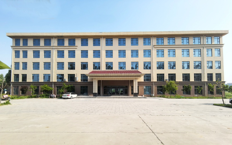
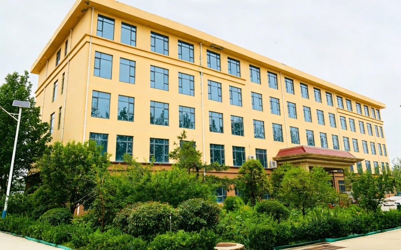
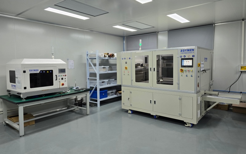
Our 20,000m² standardized production base in Hebei represents our commitment to manufacturing excellence. Equipped with advanced production lines and rigorous quality control systems, this facility enables us to deliver high-precision semiconductor equipment at scale while maintaining the exacting standards our global clients demand.
A team of 80 production engineers ensures every piece of equipment meets our stringent quality requirements before shipment. Our vertically integrated approach — from R&D through manufacturing to after-sales support — gives us complete control over quality, lead times, and continuous improvement.
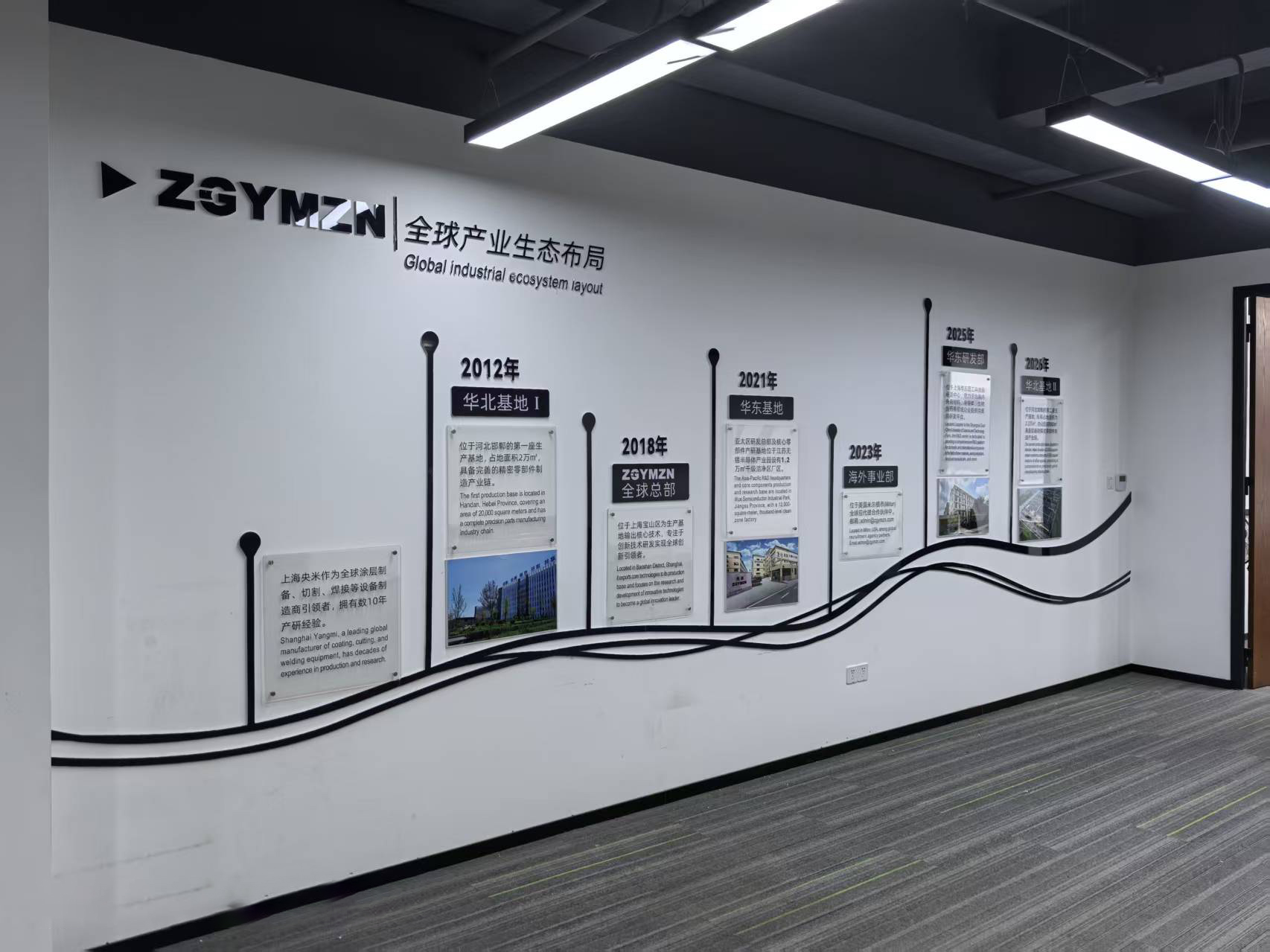
Our self-built semiconductor industrial park in Jiangsu serves as our Asia-Pacific R&D headquarters and core semiconductor component production base. This state-of-the-art facility houses advanced laboratories, clean rooms, and testing centers that drive our next-generation equipment development.
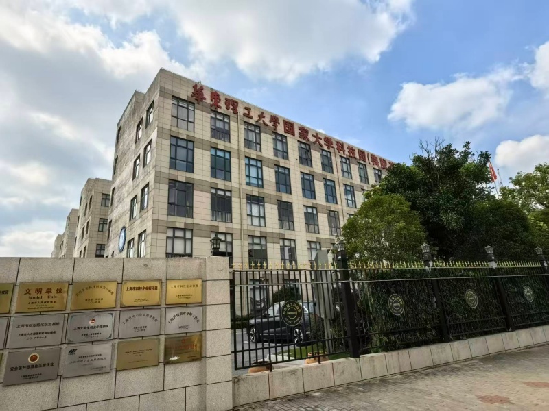
Combined with our Shanghai global headquarters and Hebei manufacturing center, this three-site collaborative ecosystem creates a powerful synergy — strategic management in Shanghai, large-scale production in Hebei, and deep technology R&D in Jiangsu. Our 40 marketing and management professionals bridge these operations to deliver seamless service to semiconductor fabs across 30+ countries.
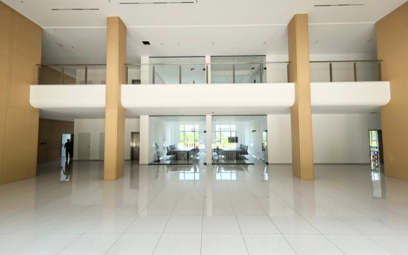
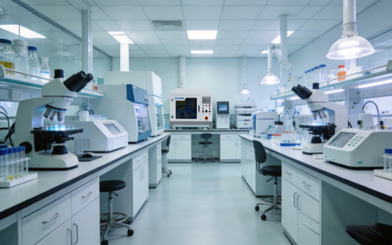
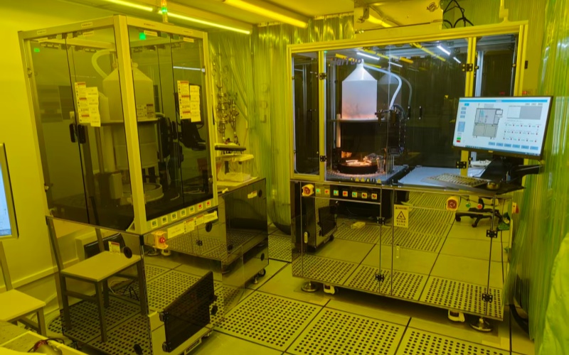
Advanced R&D labs and clean-room production facilities across Shanghai, Hebei, and Jiangsu.
We pursue world-first technologies and continuously push the boundaries of semiconductor equipment. Our 32-person R&D team is dedicated to solving the industry's toughest challenges with breakthrough solutions that redefine manufacturing possibilities.
Every piece of equipment undergoes rigorous testing at our 20,000m² production base. Our 80 production engineers ensure zero-compromise quality control from design through delivery, upholding the exacting standards our global clients demand.
With operations spanning Shanghai, Hebei, and Jiangsu, we serve semiconductor fabs in 30+ countries worldwide. Our global team of 200+ professionals provides dedicated support from initial consultation through after-sales service.
Contact our team for equipment consultation, technical specifications, or a custom solution proposal tailored to your production needs.