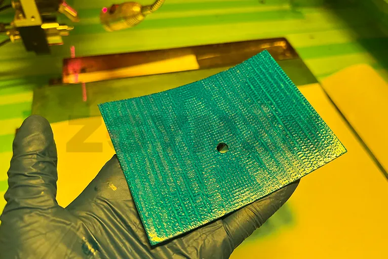
Photosensitive adhesive is a widely used technology in modern industrial production
Components and functions of photosensitive adhesive
**Film-forming agent**: It is the main component of the plate film, determining the strength, viscosity, and resistance of the film, such as water resistance, solvent resistance, print resistance, and aging resistance. Common film-forming agents include gelatin, protein, andPVA(Polyvinyl alcohol) and its modified colloids, such asPVACombined with emulsions made of non-water-soluble polymers,PVAchemically modified colloids, as well asPVA(or gelatin) combined with crosslinking agents, etc.
- **Photosensitizer**: Under blue-violet light exposure, photochemical reactions occur, causing the film-forming agent to polymerize or crosslink, which determines the adhesive's performance such as light separation sensitivity, resolution, and clarity.
**Additives**: Added to adjust for deficiencies in the performance of the main components, such as dispersants that make all components evenly dispersed, colorants that change the color of the photosensitive adhesive for easier identification, sensitizers that improve photosensitivity speed, plasticizers that increase the flexibility of the film and stabilizers that help improve the stability of the photosensitive adhesive, and so on.
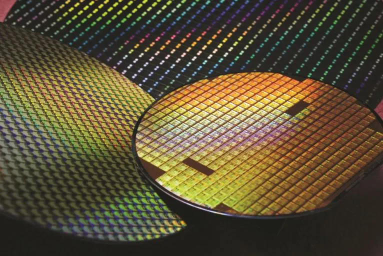
The principle of ultrasonic spraying -
The ultrasonic spraying system mainly consists of ultrasonic atomization nozzles, drive power supplies,XYZIt consists of a three-axis linkage servo system, intelligent operating system, liquid supply system, low-speed air shaping device, and casing housing.
- Its working principle is to use ultrasonic vibrations to convert liquid photosensitive adhesive into extremely fine droplets, which are evenly dispersed and adhere to the substrate surface under the influence of ultrasound.
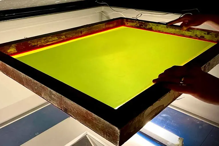
Advantages of ultrasonic spraying photosensitive adhesive
- **High coating uniformity**: The uniformity of liquid particle distribution after atomization by ultrasonic nozzles is significantly higher than that of traditional two-fluid nozzles, achieving 95%. As a result, the uniformity of the sprayed coating is greatly improved, avoiding the uneven coating distribution in high aspect ratio structures caused by surface tension issues in traditional methods such as spin coating, allowing for better filling of fine areas and preventing voids or uneven coating thickness.
- **Precisely control coating thickness**: The ultrasonic nozzle acts without pressure on the liquid and can control the flow of the coating liquid for atomization spraying through high-precision metering pumps such as injection pumps. The flow control accuracy can reach picoliters per second, enabling precise control of coating thickness, which helps reduce the amount of photosensitive adhesive, lower costs, and improve production efficiency.
- **Wide range of applications**: Suitable for various types of substrates, such as silicon wafers, glass, ceramics, metals, as well as different types of photosensitive adhesives, with broad application prospects in integrated circuit manufacturing, LCD displays, printed circuit boards, and many other fields.
- **High material utilization**: The atomization process of coating does not require gas pressurization; only a very low carrier gas pressure is applied after atomization to deliver the liquid mist, greatly reducing liquid rebound and splashing caused by high-pressure two-fluid spraying. The raw material utilization rate is comparable to that of ordinary more than four times that of air spraying, with the highest possible reach90%That's all.
- **The nozzle is not easily clogged**: Ultrasonic nozzles atomize liquids through ultrasonic oscillation. The atomized particles are determined by the frequency of ultrasonic vibration, and fine atomized particles can be produced without requiring a very small nozzle aperture. This reduces the risk of nozzle clogging and lowers equipment maintenance costs.
Application areas
- **Microelectronic semiconductors**: In chip manufacturing, photoresist coating ensures that the photoresist forms a uniform and dense coating on substrates such as silicon wafers, improving lithography quality and yield, which is crucial for producing high-precision integrated circuits, microprocessors, and other devices.
- **Photovoltaic industry**: For example, in solar cell production, photosensitive adhesive can be evenly sprayed onto the surface of the cell to form specific patterns or functional layers, helping to improve the photoelectric conversion efficiency and stability of the cell.
- **Display panel manufacturing**: On the LCD display panel, During the manufacturing process of OLED display panels and similar materials, photosensitive materials such as photoresist are applied to ensure pixel precision and display quality.
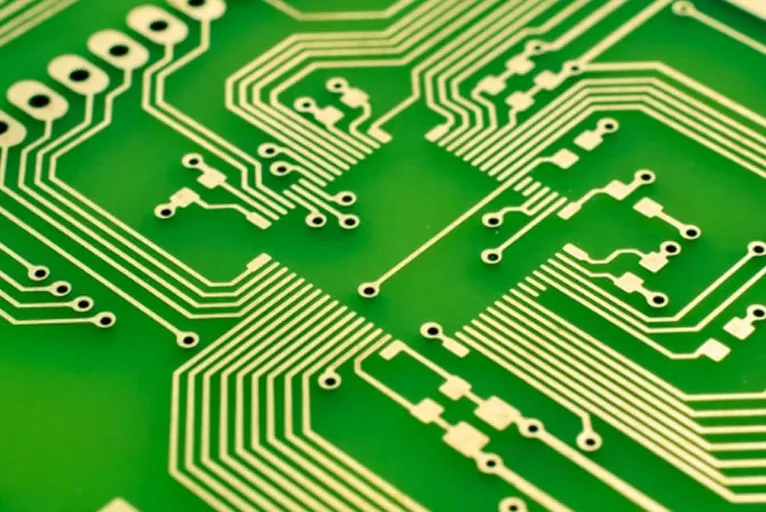
- **Printed circuit board (PCB) production**: Can precisely spray photosensitive adhesive onto PCB. After processes such as exposure and development, conductive circuits and insulating layers are formed, achieving thisPCBHigh-precision manufacturing of the board.