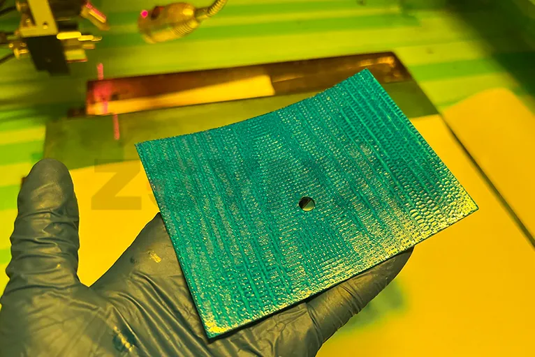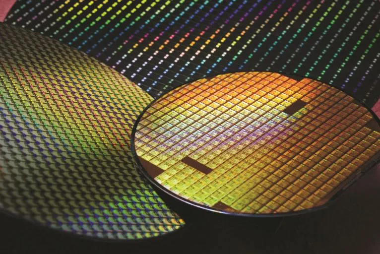

Electroluminescence (EL) is a type that directly converts electrical energy into light energy physical phenomenon. From the perspective of luminescence physics, it can be divided into low-field electroluminescence and high-field typesElectroluminescenceTwo types. Low-field typeElectroluminescenceGenerally refers to 'in'A few carriers are injected into the PN junction of III-V compounds, producing recombination and resulting in luminescence—this is the usual patternLEDs (light-emitting diodes). High-field electroluminescence is a type of high-field non-junction device that emits light from group II-VI materialsCompound。
High-field electroluminescent device structures can be divided into three types: thin-film type, thick-film hybrid type, and powder type. AC thin-film and hybrid types can be used for matrix display, which is currently the caseKey aspects of EL technology development; The AC powder type is used for this purpose, LCD and other planar light sources.
AC thin-film electroluminescent displays are fully solid-state flat panel display devices featuring the following seriesSolid-state devicesUnique features:
1. Fast response speed, reaching tens of microseconds.
2. Wide viewing angle, up to 80° ±, allowing multiple people to view simultaneously.
3. Wide operating temperature range, -55°C~+125°C, exceeding the extreme temperatures typical of integrated circuits.
4. Thin and sturdy, effective components have no cavities or sealing structures, so they can withstand loadsGlass panels can withstand various vibration and impact conditions.
Currently, semiconductor electroluminescence mainly focuses on three directions:LED (semiconductor electroluminescence), OLED (semiconductor material thin-film electroluminescence), QLED (inorganic semiconductor quantum dot thin-film electroluminescence)
YMUS ultrasonic atomization spraying technology for the preparation of inorganic quantum dot electroluminescent devices (QLEDs)
Compared with conventional spin coating processes, ultrasonic spraying technology offers three major advantages:
1.It saves materials. For ordinary spin coating processes, it exceeds the required amount during the spin coating process90% of materials are wasted, and the material utilization rate in the spraying process is highgreater than 95%;
2.Spraying technology can produce large-area devices, whereas spin coating technology cannot. This makes spin coating technology impossible to apply in industrial production.
3.Conventional spin coating technology cannot mask devices to create pixels, whereas spray coating technology is fully compatible with mask processes.
YMUS spraying technology is low-cost and efficient solution-based thin film preparation process,It is applied in industrial production.
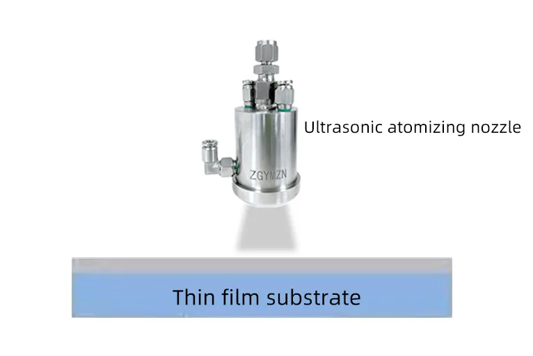
Schematic diagram of ultrasonic atomization spraying
Different thicknessesAFM image
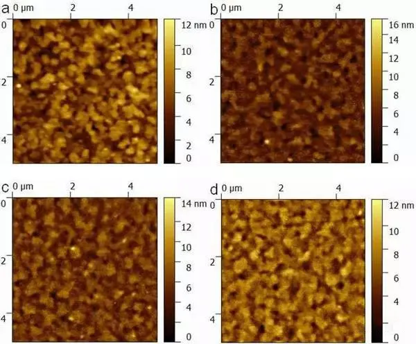
(a) Deposition of Al of different thicknesses2O3Behind the floorSurface morphology of NiO;
(b) 2nm;(c) 5nm;(d)8nm。
Using ultrasonic atomization spraying technology, inorganic quantum dot electroluminescent devices are prepared (QLEDs), which have played an excellent role in the development of inorganic QLED device research, and YMUS is providing even better technical services for the production of high-quality quantum dot electroluminescent illuminator display devices.